
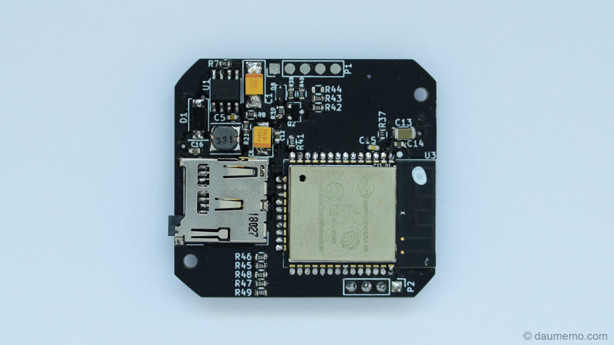
Today I will talk about several problems I had after designing a custom PCB for an ESP-32 module. This PCB was used in Wi-Fi connected switch used for controlling LED strip Wi-Fi enabled module.
The idea was to make a PCB for a Wi-Fi switch. The switch itself was modified commercially available wall switch made by italian manufacturer BTicino. It would connect to a Wi-Fi LED strip controller which I talked about in my older post. Also, the board was made in such way that it could be used with six or four button switches. When used with four buttons – one third of the board needs to be cutoff.

How everything is connected you can see in the schematic. All board is powered from a 12 volts power supply placed on a secondary board. Note, that component placing in the schematic might seem very messy as it was iterated several times without cleaning up afterwards.

A problem with IC’s power
After I have soldered everything to the PCB and connected it to a power supply – nothing happened (the ESP-32 was powered off). So, first logical step was to check if everything’s OK with PSU voltages. There was 12 V voltage before MC34043 DC/DC converter IC and after it there should be 3.3 V, but it was only around 2 Volts. Also, it seemed as if the converter was constantly switching itself on and off.
The cause of the problem sorted out after pushing the ESP’s reset button. I have noticed that when I push and hold the reset button – the voltage after the DC/DC converter raised to a normal voltage of 3.3 Volts. So, it seemed that DC/DC converter had been limiting maximum current during ESP’s startup.
A resistor (in this schematic R7) is responsible for current limiting. Its value of 1.5 Ohms was chosen. This value sets current limiting to around 200 mA. Which, apparently, was not enough. So, I have changed it to 1 Ohm resistor, and it worked – the voltage after the DC/DC converter was constant 3.3 Volts. When ESP is in reset state (reset button is held down), it draws little current, so DC/DC converter the can output normal voltage.
Bootstrap pins
But the overall problem wasn’t resolved. Although ESP was powered from a needed voltage, it still wouldn’t boot up normally. You may ask, how do I know if it boots normally or not? Well, the firmware which was flashed into ESP should have started its own Wi-Fi access point, but it never did. The firmware code was without any bugs or mistakes as it was tested on a regular ESP dev board and it worked fine. So, everything shows that ESP on a custom PCB won’t boot up into normal operation mode…

First thing to do was to check if the PCB was designed correctly and if all special boot pins are pulled up/down correctly during the boot process. You might say that ESP-32 has internal pull-up/down resistor which defaults to needed normal boot process and you will be correct. But in this case, some of those pins are connected to either LEDs or buttons (more about that later). So, looking to the schematic I firstly desoldered R14 and R17 resistors as they connected bootstrap pins to LEDs which could have pulled up bootstrap pins incorrectly. This didn’t help… So, it needed a second look trough.
The IO0 pin
The second idea was that maybe for some reason I haven’t flashed correctly the ESP. I tried to do the flashing the second time I noticed that it flashed itself without the need to get the ESP into flashing mode. As this mode should be entered holding SW2 button during power up, but as mentioned, the chip entered the flashing mode without holding the button down. So, I looked up the datasheet and it was clear that the problem must be with an IO0 pin as it is responsible for setting the chip into flashing or normal boot modes.
The IO0 pin was connected to the SW2 button and pulled up with the R48 resistor. Which was and is correct connection. So, how could it be that even when it is connected correctly the chip boots into the wrong mode? There is another component connected to the same pin and it is the C3 capacitor. Together with the R4 resistor it makes an RC circuit which should filter out some of the contact bouncing during the button press. But as it turned out the C3 capacitor was the root of the problem, because after desoldering it – the ESP booted normally.
So, how the C3 capacitor was at fault? Logically, when the ESP gets power it waits for the EN pin to rise high. When it rises high it checks bootstrap pins and boots into a defined mode by those pins. What happened here is that voltage on the IO0 pin was rising slowly because of the C3 capacitor and the EN pin got HIGH faster than IO0 pin which then was read as LOW. After desoldering the C3 capacitor, the IO0 pin always gets HIGH before EN pin starting up the whole chip.
Awkward LED connection
You may ask why I thought that connecting LEDs to bootstrap pins was a good idea. Well, it wasn’t. On the first iteration of the board schematic I have chosen to use more LEDs in total and I ran out of available IO pins. So, I used a LED driver IC which inputs had high impedance and everything should have been OK. After seeing that additional chip takes a lot of board space, I have removed that IC and some LEDs, but haven’t though than in this new situation LEDs will be directly connected to the bootstrap pins and will probably have a great impact on device’s boot process. So, I have made a mistake again.
As I have mentioned, I desoldered two resistor to physically disconnect two LEDs from bootstrap pins. I wanted to leave those pins as they were at that point disconnected, but also, I wanted to be able to use those disconnected LEDs. Thus, I have decided to physically connect LEDs to other ESP pins which were intended to be used (if ever needed) for optional I2C connection. As you can see in the photo below, I have used some thin wire to do the physical connections.

Power fail detection circuit
There is also a circuit responsible for notifying ESP during power failure when the voltage before DC/DC converter went down. It consists of components D8, R38, R39, R40, and Q2. In theory, when there is a voltage before DC/Dc converter (on D8, R38 and R39), the transistor pulls ESP input LOW. When the power fails, the Q2 closes and R40 resistor pulls ESP input HIGH.

At first this circuit was not operating correctly. I have found out that R39 value was too low and the voltage on transistor base was always too low to fully open Q2 and pull the ESP’s input low. After changing the R29 resistors value from 6.8k to 11kOhms, it started to work properly.
There is one noticeable thing about this circuit and ESP itself. It seems that there is enough time to detect power failure and do something simple, for example, to switch on a LED before power down. But it seems that there is not enough time to do complex tasks. I have tried to write something to a SD card before power failure, but after every power down nothing was written to the SD card. This circuit was intended to save some settings to the ESPs memory before power failure and then to retrieve those settings during new boot. It might be possible to do that with emulated EEPROM, but I haven’t tried it. So, either I will test it with an EEPROM at some time or this function will be never used…
Final thought
Although it might seem that all problems were solved as fast as you have read trough this posts text, but, in reality, it took like two days to do that. I hope, this situation will be informative to some how not to do some things and successfully design a PCB for an ESP-32 chip.
Gallery