This tutorial is about an UV exposure method for making you own PCBs in home environment. This method allows you to etch boards suitable even for tiny SMD components (except maybe for BGA parts). Although it takes some effort, making PCBs at home allows you to design, make, solder and test prototypes faster than ordering the boards from PCB manufacturers.
Disclaimer
First of all, I wanted to say that you should take all possible safety precautions when dealing with chemicals. Some have strong odor, so you should always work in well ventilated room.
For protection, use gloves, respirator and if needed eye protection.
Always follow the instructions and precautions, written on the chemical labels. Do not ingest chemicals used in this tutorial.
It is your responsibility to keep yourself safe during whole PCB making process!
Table of contents
- Short version of a whole PCB making process
- Materials explained, alternatives
- CAD software settings, design parameters
- Making PCB image
- Cutting the board to the needed size
- PCB exposure under the UV light
- Dissolving unneeded photoresist
- PCB etching
- Drilling holes
- Cleaning and VIA soldering
- Summary
Short version of a whole PCB making process
In short, when making a PCB at home via UV method, the following steps need to be made:
- Print a “mask” on a semi-transparent paper (or a transparent film) which will block the UV light were the traces need to be.
- Cut a needed size PCB which also has a photoresist layer on top of a copper layer.
- Align the mask on top of the PCB.
- Expose the PCB with the mask under the UV light.
- Develop the traces in chemicals (unneeded photoresist parts are washed away).
- Etch the PCB in the etching solution (only copper traces will be left).
- If needed, drill holes and vias.
- Solder vias (connect two layers together if double-sided PCB is used).
All steps are explained in-depth in the following paragraphs. If you wonder if there are other methods of making PCBs – there are. Previously I have talked about DIY PCBs with a CNC router. Of course, you could get the PCBs professionally manufactured.
Materials explained, alternatives
Material, part list:
- Semi-transparent paper (or a transparent film)
- UV lamp (might require a ballast or a driver – depends on the lap’s type)
- Some cardboard box for placing the UV light
- Inkjet or laser printer
- Some clear sticky tape
- Plexi-glass (4 mm or thicker)
- PCB with positive photoresist layer (single or double-sided)
- Metal cutting saw or alternatives for board cutting
- Some sanding paper, a file
- Gloves, respirator, other safety equipment
- Acetone
- Jar, container for chemicals
- PCB positive photoresist developer chemicals
- PCB etching chemicals
- Some insulated wire for hanging the PCB in the etcher
- Tweezers
- Soldering flux, solder, soldering iron, other soldering tools
- Drilling tools: an electric drill or a Dremel, drill bits
Materials explained
I personally use semi-transparent paper because my laser printer does not want to print good quality prints on a film. So, it is up to you to find out what works best for you. The paper can be found at any office supplies selling shop.

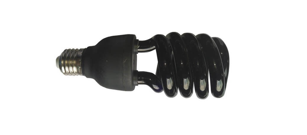
UV lamp might be as simple as shown below. It will require additional wiring + a switch to power it for a needed period of time. The lamp should be placed into some kind of box (probably cardboard), so the whole assembly would become an UV box for exposing the PCBs. It will also prevent from UV direct contact with your eyes.
A clear sticky tape will be used to hold the paper mask on the PCB as well as holding several paper mask layers together. A sheet of plexi glass is used to hold in place the paper mask flush with the PCB surface. Also, the plexi glass passes through UV rays. It is better to have thicker plexi, because it won’t bend as much as the thinner ones.
PCBs, chemicals
PCB with a photoresist layer should be bought from a local electronics shop. There you will also find chemicals needed: a developing and etching solutions. Developer and etcher are shown below:


As an alternative for the developer NaOH (Sodium hydroxide) can be used. Is is usually used as a drain cleaner. It is the best if this solution is in dry state than a liquid as it will be easier to mix it with water. What the ratios should be it is again for you to experiment and find out. Because this alternative adds additional variable to the whole process, for the first time I would recommend sticking with the developing solutions found in electronics shops.
For PCB etching I use Sodium Persulfate. I don’t know any alternatives for it. Iron (Ferric) chloride might be used as alternative, but recently it became hard to find, at least in my country.
Other materials
If you are making your own PCBs, you will probably have all soldering materials needed to cover the PCB with solder, solder vias (if needed), clean the board after etching/soldering (acetone).
You will need a drill with drill bits to make some holes in the board. For this purpose, I would recommend using some kind of drill press or a Dremel holder as I do. Carbide drill bits are the best, but they break easily, especially if drilled with handheld tool. HSS bits can be used with handheld drill, but they will get dull faster.
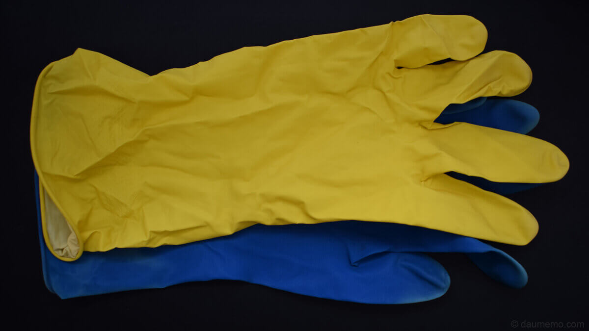
Finally, you will need safety equipment. Use rubber gloves, safety glasses and respirator (especially if you are going to use NaOH). Work in a well ventilated room.
CAD software settings, design parameters
The main thing to note before trying to make a DIY PCB is that these PCBs won’t have any plated holes (in contrast to professionally manufactured boards). Which means that if you’re making a double-sided PCB, both layers need to be soldered together using thin wires. Of course, if a single-sided PCB is being made, there won’t be any problems with two layers interconnection.
The minimum track width that is manageable with UV method – 0.2 mm. Although it is possible to get such tiny widths manufactured at home, I still suggest going with as wide tracks as possible – it will make your life much easier. And if you still need tiny tracks – make them as short as your design allows.
Also, minimum hole/via drill size should be >= 0.5 mm. I usually use via pad diameter of at least 1.2 mm. Again, the bigger, the better, as it will be easier to solder wires/parts on bigger copper pads.
Keep in mind that copper layer in the end might be etched down to a smaller widths/sizes than they actually are in the design software.
Making PCB image
One of the first steps of the actual PCB making is to print an UV mask on a semi-transparent paper (or a transparent film). The idea is simple – the UV mask covers those PCB areas where the traces need to be while other places will be exposed to the UV light.


I would recommend using double mask. That means for each PCB copper side you will have to print two same PCB trances pictures. Then alight them and stick together with a clear sticky tape. Such double mask will help to improve image quality – at least my printer tends to print the traces not black enough, so UV light gets through the black areas. Aligning two image layers makes the traces less transparent to the UV light and improves overall PCB quality.
Of course, you could get away with only single layered mask, but the PCB traces might get “eaten away” by the etching solution if they get some UV light. You can see how “thin” ink on a single sheet of paper looks like:

When you put to layers of paper together, you will get much darker tracing view:

The top PCB layer needs to be printed mirrored, while the bottom layer – not.
Single-sided PCB will use one “double” mask – you need to print two same layer images and put them together. Double-sided PCB will require two “double” masks, so you will have two layer images printed each twice.
Here are some schemas, showing how to put those masks on a PCBs:


Both masks for double-sided PCB needs to be aligned together to form a “pocket” which you will put the PCB into. In all cases, the mask ink should face to (not from) the copper layer.
This is how a “pocket” for double-layer PCBs looks like:


Cutting the board to the needed size
Usually, the whole board which you buy from a shop will be bigger that it actually needs to be for your application. Obviously, then the PCB needs to be cut to a needed size.
If the board is double sided, then it is best to have it a little bigger at least on one of its sides, so the PCB image printed on a piece of paper can be held by a transparent sticky tape. After whole etching process it then can be trimmed down to exact dimensions or left untouched if bigger measurements are acceptable. Moreover, if your board is single sided, then it can be cut to the exact dimensions from the start.
I personally for the board cuts use a metal cutting saw. Just measure in your CAD software what the size of the board needs to be, draw the outline with a pen on a PCB and cut it with a saw.

After you cut out the PCB, you might end up with rough edges, especially on those sides where the copper layer is. Because of these rough corners, your PCB might not lay flat on its surface, so you should file those rough corners down:

In single sided board case, you will have a board which one side is covered with a positive photoresist. This side will also have a protective film (blue tape) which needs to be peeled off before exposing it to the UV light.
In double sided PCB case, you will have both PCB sides covered with photoresist. Also, both sides will have a protective layer which needs to be peeled off before UV exposure.
PCB exposure under the UV light
This step is quite straight forward. If you have a double-sided PCB, you have to put it inside the “mask pocket” which was made in previous steps. If you have a single-sided PCB, you will need only to put the PCB on the mask paper and press it down with some weights. Here is shown how the double PCB’s and Mask’s “sandwich” looks like:

Note, that in this step all protective covers (Blue tape) is removed. At this stage work very carefuly and try not to scratch the PCB surface.
And here is a schematic, how you should put masks, PCBs and UV lights together in a simple UV box to get the needed result:

Now, put the PCB according to the one of the schematics above. How long to keep the board under the UV light is up to you to decide. It will depend on the light’s strength and the distance between the light and PCB. So, you will have to test it with several boards with different times and see what UV time gets the best result.
My personal UV exposure time is about 5 minutes for one PCB side.

In case of double-sided PCB, remember after keeping one side under the UV light to flip the board, so both sides would get the UV exposure.
Dissolving unneeded photoresist
To dissolve unneeded photoresist parts and leave the traces intact, you will have to use a developer solution. When bought from an electronics shop it needs to be mixed according the instructions.

I usually keep the developing liquid in the plastic container and put the PCB into the solution with tweezers. If the PCB is single sided, it can be left on the bottom of the container. If the PCB is double-sided, you will have to hold it with tweezers submerged into the liquid, but without touching the container’s bottom. Otherwise, you might scratch the PCB’s surface an it could end up with some traces being cut off when etching.
Mostly I keep the PCB submerged into chemicals for 0.5 – 2 minutes. The exact time will depend on how old the developing chemicals are. It is best to frequently get out the board from the liquid, rinse it under the running tap water and see if unwanted photoresist is washed away. If not, put the board into the developer again and repeat the process till you will clearly see the traces.
The view after all unwanted photoresist is washed away:

PCB etching
For PCB etching I use Sodium Persulfate. It comes as a porous solution in a small bag which needs to be solved into water.
From 100g of Sodium Persulfate you can get about 0.5 liter of etching solution. Of course, the packaging might be different where you live in, so always mix the solution according to the included instructions.
I keep the etching solution in a glass jar. It is written in the instructions that the solution needs to be warm (but less than 50 C). It will be warm if you mix the solution first time with warm water. Obviously, it eventually will get cold. For the following PCB etchings, you should warm up the solution, because when it is cold it will take a lot of time to etch a PCB.
After developing the board in chemicals (as written in previous step), it is best to drill a small hole which will be used to hang the board inside the etching jar.

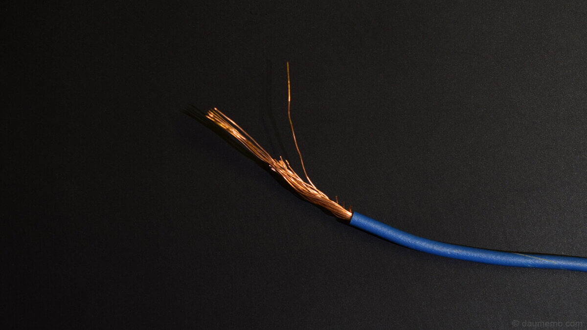
Then, hang the PCB with a piece of wire into the jar. For this purpose, I use enameled wire, so the etching solution will not dissolve it. Probably any wire with plastic coating/insulation will be suitable.
Depending on how new your etching solution is, it might take from 20 minutes to 2 hours to fully etch the board. I usually check how the process goes every 15 minutes and if I see that all (or at least most) of unwanted copper is dissolved, I take out the PCB from the jar and rinse it under the running tap water. While rinsing you can use some soap to clean the board. Finally, I dry the board with a paper towel.
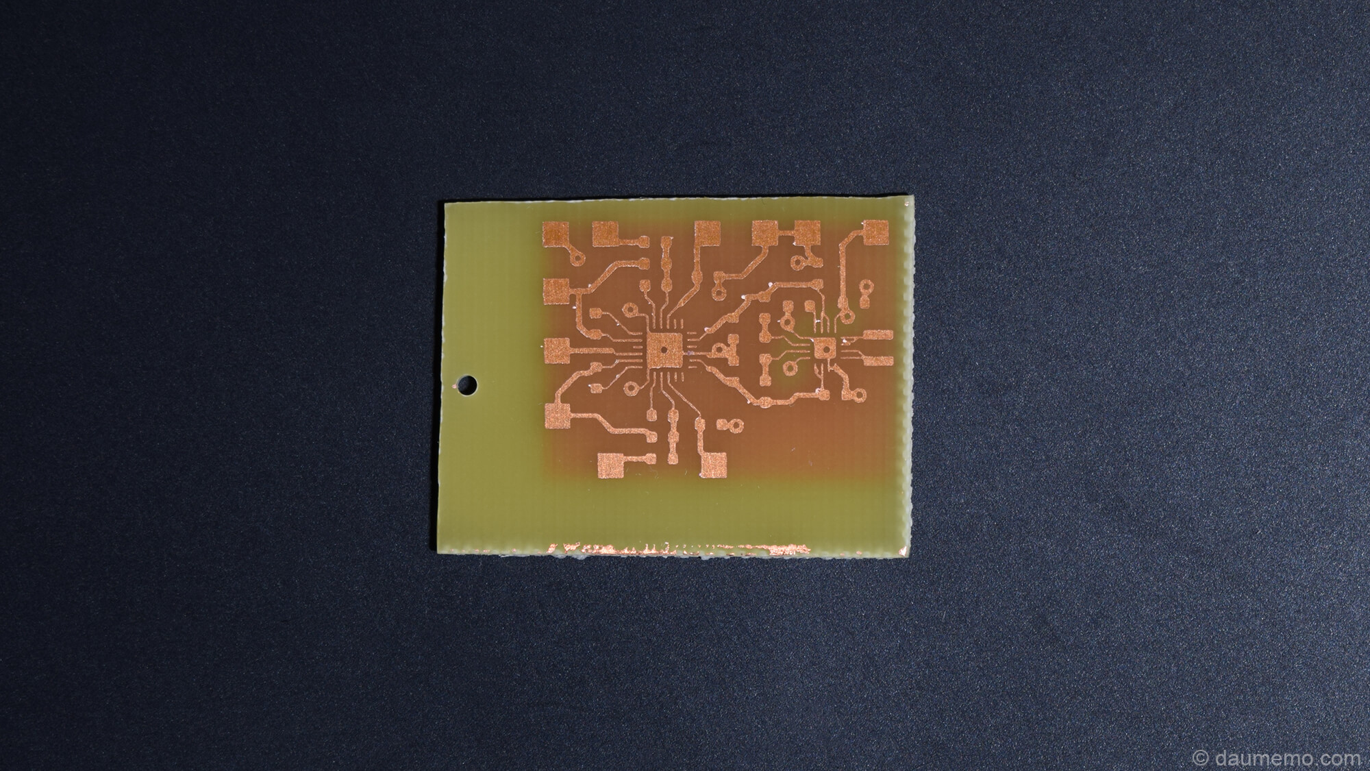
After this whole process, you should be able to clearly see the PCB traces:

The following step is to drill the holes (if your board design requires it).
Drilling holes
Drilling holes in a PCB might look like an easy task, but in reality, it isn’t.
I personally use carbide micro drills, such as show below in a photo:

Although, you could try to use them with a regular electric/battery powered drill, you will probably end up breaking all the bits without drilling any holes. These bits are very brittle, so you will have to use some kind of stationary drilling machine or a drill stand. I use a 3D printed rotary tool holder, which makes drilling a lot easier:

I have also tried to drill the holes with some 0.5 – 1 mm diameter HSS drill bits. These can be used (carefully) with a handheld drill as they are not as brittle as the carbide ones. The problem with HSS bits is that they tend to get dull quite fast, but still, it can be an option if you don’t have any alternatives.

Of course, drill bit diameter needs to be chosen according to PCB hole sizes used in your CAD software.
Because I use KICAD, it has an option to set drill holes on a printed mask to small dots instead of real diameter holes. This option makes it easier to align drill bit tip to the hole’s center.
Here is a PCB with already drilled holes:

Cleaning and VIA soldering
To clean photoresist layer from the board, I use acetone. I usually clean the board with acetone when all processes – development, etching and drilling – are done.
I have average size plastic container into which I pour some acetone. After that, I just put the PCB into the container with acetone.
Note, that you should test the container before use if it does not melt from a reaction with acetone.
After several minutes acetone will strip off the photoresist layer. Additionally, you could rub the PCB with some paper towel to fully clean all residues from the board surface.
Although optional, I would recommend to cover the copper layers with a thin solder layer, so it will be easier to solder the parts onto the board:

If your board has two layers you will probably end up having some vias. Of course, they will not be plated with copper as the professionally made ones. To connected both DIY PCB layers you will have to solder both vias sides together with a thin wire. I usually take the thin single strand from a stranded wire, but you could use anything that physically fits into the drilled vias hole (like thin resistor leads etc.).

The final result of the DIY PCB made at home:

Summary
So, this is quite sophisticated method, how you can make a DIY PCB with quite small traces for most SMD components. Although this method requires quite a lot of patience and workmanship, but in the end, it is a workflow which allows you to test you own PCB designs in shortest possible time – the PCB from the design till the soldered board could take 2-4 hours (depends on your skills and board complexity).