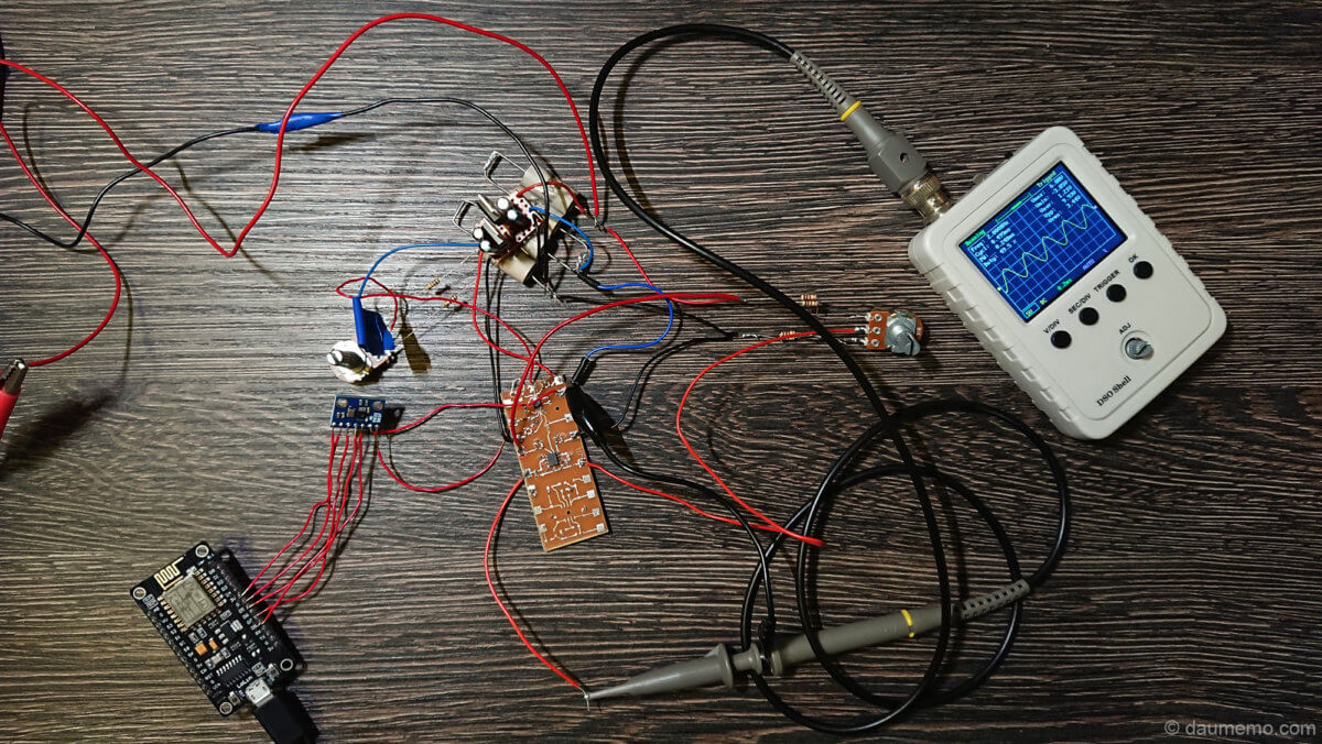
In this post I am going to continue with the DIY signal generator based on the AD9833 IC where I have left in the previous part. Earlier, I have talked how I had built my first analog signal generator’s stage – variable gain amplification circuit. Usually, a generator needs to have an ability to change not only the signal’s amplitude, but also its offset. So, today I will walk you through a circuit which adds an offset to the DIY generator’s output signal.
Let’s remember full circuit which was shown in the first part:

Links to project’s all posts
- VCA822 Gain Amplifier Circuit
- LM7171 Offset Circuit (this post)
- Gain and Offset Control Filter Circuit
- Dual 5V Power Supply
- Dual 12V TPS65131 Power Supply
- Battery Charging Circuit with BQ24295
- Basic WEB Interface
- IPS Capacitive LCD on an ESP32
- IPS LCD, ESP32 with eSPI library and Touch screen
- Final PCB Design for the DIY Waveform Generator
- Custom Design PCBs and How To Get Them Manufactured
- Soldering the PCB
- AD9833 Library and Further Output Noise Reduction
- Arduino BQ24295 Battery Charger Library
- LCD GUI with LVGL on ESP-32
- 3D Printed Enclosure
- Finished DIY generator
The LM7171 Circuit
Today we will look into a LM7171 op-amp’s circuit:

Capacitors C12 and C15 were chosen to be 1uF each, capacitors C13 and C14 – 100nF each. R15 was chosen to be 100 Ohms as with such load manufacturer made most of the specification measurements. R15 value might be changed in the final design, because in the end, this generator needs to be battery powered and such load increases total power consumption. Although higher resistance could (or not) induce additional problems in higher frequencies as the line between op-amp’s will be with unmatched load. Unfortunately, I don’t have a good oscilloscope to test it at this moment, so let’s just make this circuit to operate in lower frequencies (sub 100 kHz) and then we will se what to do about high frequencies.
R16 value is 0 Ohm, it was also tested with 100 Ohm resistance. Its main purpose to counterbalance the resistance on the second input and also to minimize output offset. Because LM7171 circuit is used for adding and controlling the offset – R16 becomes not so important.
Values for R17 and R18 were chosen respectively 100- and 390-Ohms giving gain of 3.9 (although I wanted to have gain of 4, but it is good enough for initial testing). Also, C11 was omitted (might be used for limiting the output bandwidth in the future).
The New PSU Circuit
I also have made some changes to the power supply circuit because I needed several supply voltages: +- 5V for VCA822 and +-12 V for LM7171. So, let’s look into a newer PSU schematic:

Here, the resistors R1, R2, R3 and R4 are used to make virtual ground point. Additionally, to make +- 5V power supply for the VCA822 chip, 7805 and 7905 voltage regulators were used. Also, R6, R5 and potentiometer RV1 makes a circuit to control the offset on the LM7171 output. RV1 outputs around +- 1V into 100 Ohm load.
The Result

After connecting everything together and powering it up, to my surprise, I’ve got the result that I wanted to get. By turning one potentiometer – output signal’s amplitude changes and when I turn the second potentiometer – signal’s offset changes.
Everything works except for minor one thing – when turn up the gain somewhere more than 50%, the output signal gets distorted. When I put my hand on the oscilloscope’s cable, the distortion disappears. It seems that it is not circuit’s problem, but the problem lies either in the scope itself or in its probe cable…

Lastly, I have measured several signal generator’s output parameters (note: measured with the DSO150 scope):
- Output voltage saturation is + 10.6V and -10.4V when powered from a +-12V power supply
- Maximum offset value: +4.5V
- Minimum offset value: -4.7V
- Signal’s (sine wave) peak voltage with maximum gain: 18.4Vpp (with 0V offset, no voltage saturation)
Summary
To sum up, everything went perfectly with the second DIY signal generator analog stage. Output values are almost those that I personally want to get (I would like to get 20Vpp max output amplitude which is easily achievable). The only thing to investigate in the future – the signal distortion and its disappearance when probe cable is held in the hand.
So, in the next part I am going to build filter circuit which should convert PWM signals from an MCU to DC voltages that are needed to control offset and gain (and get rid of both potentiometers).


