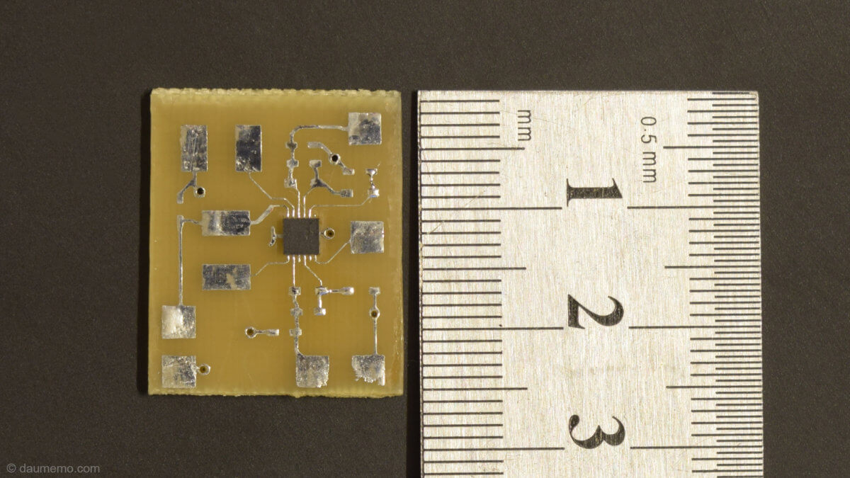
Today’s continuation of the DIY signal generator based on an AD9833 is going to be about a dual rail 5V power supply. In the first part I have introduced you to a variable gain amplifier stage. The power supply is going to be used to power the mentioned operational amplifier.
Links to project’s all posts
- VCA822 Gain Amplifier Circuit
- LM7171 Offset Circuit
- Gain and Offset Control Filter Circuit
- Dual 5V Power Supply (this post)
- Dual 12V TPS65131 Power Supply
- Battery Charging Circuit with BQ24295
- Basic WEB Interface
- IPS Capacitive LCD on an ESP32
- IPS LCD, ESP32 with eSPI library and Touch screen
- Final PCB Design for the DIY Waveform Generator
- Custom Design PCBs and How To Get Them Manufactured
- Soldering the PCB
- AD9833 Library and Further Output Noise Reduction
- Arduino BQ24295 Battery Charger Library
- LCD GUI with LVGL on ESP-32
- 3D Printed Enclosure
- Finished DIY generator
The Device
So, the signal generator is going to be a battery powered device. This means, that power IC must work with 3 to 4.5 V input voltage. It also has to deliver at least 50 mA of current on both rails. Finally, output voltages need to be around +5V and -5V.
With those requirements ON Semiconductor’s LV52117QA chip was chosen. It is designed to deliver dual 5V with up to 100mA output current. It is also quite cheap solution: the IC itself costs around 2 USD and it requires only bare minimum component count. The only and main problem with this chip is that it is very tiny. Which, on one hand, is good as it takes not much space on a PCB, but, on the other hand, it is very difficult to solder at home…
After deciding on which IC to use, I have made a schematic for a test PCB:

As you can see it is the same schematic as shown in the chips datasheet. There is actually not a lot to talk about, maybe one thing I could note – LV52117QA has integrated synchronous circuit, so there is no need to have additional MosFets on board, which further minimizes whole circuit. Also, instead of suggested by the datasheet 50 kOhms (R2) resistor, 51k was used (as I didn’t have 50k at hand).

This PCB was made by me at home. I have written a tutorial how it can be done either by etching with chemicals (used in this case) or with a CNC router.
Board measurements

So, I have tested the board with dual 100 Ohm load and dual 47 Ohm load, and got such input/output values:
With 100 Ohm load:
- Output voltage U1 = + 4.84 V
- Output voltage U2 = – 4.97 V
- Battery current I = 146.7 mA
- Battery voltage U = 3.72 V
With 47 Ohm load:
- Output voltage U1 = + 4.8 V
- Output voltage U2 = – 4.94 V
- Battery current I = 347 mA
- Battery voltage U = 3.508 V

From these values, converters efficiency can be calculated – it is around 88 % at 100 Ohm and 83 % at 47 Ohm load. Which is actually not bad at all. Note, that this efficiency will depend on inductor resistance, in this case these 4.7 uH inductors were used. As they are a bit overkill for this converter in the future I will use something smaller in size.
Also, as I have used 51k resistor instead of recommended 50k, positive output voltage was a bit lower than it should have.
So, this circuit will supply variable gain amplifier stage with a VCA822 and in another part I should talk about dual 12V power supply for the offset control stage.


